
Transistor
- The transistor was invented in 1948 by John Bardeen, Walter Brattain and William Shockley at Bell Laboratory in America.
- A transistor is basically a silicon or germanium crystal containing three separate regions.
- It can either be n-p-n-type or p-n-p-type.
- It has three regions.The middle region is called the base and the two outer regions are called the emitter and the collector.
- Although the two outer regions are of the same type (n-type or p-type), their functions cannot be interchanged. The two regions have different physical and electrical properties.
- In most transistors, the collector region is made physically larger than the emitter region since it is required to dissipate more heat.
- The base is very lightly doped, and is very thin.This is because the number of carriers in the base should be small so that only small combination of hole-electron may take place in it & the collector current may not decrease considerably (i.e. the charge carriers constituting emitter current may pass on comfortably to the collector region).
- The emitter is heavily doped.
- The doping of the collector is between the heavy doping of the emitter and the light doping of the base.
- The function of the emitter is to emit or inject electrons (holes in case of a p-n-p transistor) into the base. The base passes most of these electrons (holes in case of p-n-p) onto the collector.
- The collector has the job of collecting or gathering these electrons (holes in case of a p-n-p) from the base.
- A transistor has two p-n junctions. One junction is between the emitter and the base, and is called the emitter-base junction, or simply the emitter junction. The other junction is between the base and the collector, and is called collector-base junction, or simply collector junction.
The schematic representations of a n-p-n and p-n-p transistors are shown in the figure.

The symbols for n-p-n and p-n-p transistors are shown in the figure below.

.gif)
.gif) is emitter current
is emitter current
.gif) is base current
is base current
.gif) is collector current
is collector current

In operation of a transistor,
.gif)
where,
.gif) is emitter current
is emitter current.gif) is base current
is base current.gif) is collector current
is collector current
A transistor can be operated in any one of the following three configurations :
1. Common emitter (CE)
2. Common base (CB)
3. Common collector (CC)
Input Characteristics of a Transistor
The variation of the input current with the input voltage for a given output voltage is known as input characteristics of a transistor.<
/span>
Output Characteristics of a Transistor
The variation of the output current with the output voltage for a given input current is known as output characteristics of a transistor.
Action of a Transistor
1. Action or Working of n-p-n Transistor

- The emitter-base junction of n-p-n transistor is forward biased whereas the collector base junction is reversed biased.
- When emitter-base junction is forward biased, electrons (majority carriers) in the emitter are repelled towards base.The barrier potential of emitter-base junction decreases and the electrons enter the base.
- About 5% of these electrons combine with the holes in the base region resulting in small base current (Ib).The remaining electrons (95%) enter the collector region because they are attracted towards the positive terminal of the battery connected with collector-base junction.
- For each electron entering the positive terminal of battery connected with collector-base junction, an electron from the negative terminal of the battery connected with emitter-base junction enters the emitter region.
- Thus continuous flow of electrons from emitter to collector through the base begins.
- The emitter current is more than the collector current.
2. Action or Working of p-n-p Transistor

- The emitter-base junction of p-n-p transistor is forward biased whereas the collector-base junction is reverse biased.
- When emitter-base junction is forward biased holes (majority carriers) in the emitter (p-region) are repelled towards the base and diffuse through the emitter-base junction.
- The barrier potential of emitter-base junction decreases and the holes enter the n-region (i.e. base).
- A small number of holes (5%) combine with the electrons of n-region resulting in small base current.The remaining holes (95%) enter the collector region because they are attracted towards the negative terminal of the battery connected with the collector-base junction.These holes constitute the collector current.
- The collector current (Ic) is less than the emitter current which is constituted by all the holes moving towards the base.
- As one hole reaches the collector, it is neutralized by an electron from negative terminal of the battery.As soon as one electron and a hole get neutralized in the collector,a covalent bond is broken in the emitter region.The electron-hole pair is produced.
- The electron released so enters the positive terminal of the emitter-base battery VEB and the hole moves towards the collector.
- Thus, a continuous flow of holes from emitter to collector through the base begins.
In a transistor circuit, the reverse bias is high as compared to the forward bias. Explain why ?
Ans. The reverse bias is kept very high as compared to the forward bias so that it may exert a large attractive force on the charge carriers to enter the collector region.
- A transistor has two junctions i.e. Emitter-Base junction and a Collector-Base junction.There are four possible ways of biasing these two junctions as shown in the table.
|
Condition
|
Emitter-Base junc
tion |
Collector-Base junction
|
Region of operation
|
|
1. FR
|
Forward biased
|
Reverse biased
|
Active
|
|
2. FF
|
Forward biased
|
Forward biased
|
Saturation
|
|
3. RR
|
Reverse biased
|
Reverse biased
|
Cut off
|
|
4. RF
|
Reverse biased
|
Forward biased
|
Inverted
|
- In condition 1,where Emitter-Base junction & Collector-Base junction are forward and reversed biased respectively.This condition is often described as forward reverse (FR).
Transistor as a Switch
When the transistor is used in the cut off region or saturation region, it acts as a switch.
Transistor as an Amplifier
When the transistor is used in the active region, it acts as an amplifier.
COMMON EMITTER AMPLIFIER
In the common emitter transistor amplifier, the input signal voltage and the output collector voltage are 180° out of phase.
dc Current Gain
It is defined as the ratio of the collector current () to the base current ().
.gif)
) to the base current ().
.gif)
ac Current Gain
It is defined as ratio of change in collector current (.gif) ) to the change in base current (
) to the change in base current (.gif) ).
).
.gif)
Voltage Gain
It is defined as the ratio of output voltage to the input voltage.
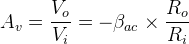.gif)
.gif)
Where, Ro and .gif) are the output and input resistances.
are the output and input resistances.
Negative sign represents that output voltage is opposite in phase with the input voltage.
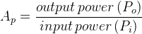
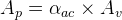
Power Gain
It is defined as the ratio of the output power to the input power.
.gif)
.gif)
.gif)
.gif)
Note : Voltage gain (in dB) = .gif)
.gif)
=.gif)
.gif)
Voltage gain (in dB) = .gif)
.gif)
COMMON BASE AMPLIFIER
In common base transistor amplifier, the input signal voltage and the output collector voltage are in the same phase.
dc Current Gain
It is defined as the ratio of collector current (.gif) ) to the emitter current (
) to the emitter current (.gif) ).
).
.gif)
.gif) ) to the emitter current (
) to the emitter current (.gif) ).
)..gif)
ac Current Gain
It is defined as the ratio of change in collector current (.gif) ) to the change in emitter current (
) to the change in emitter current (.gif) ).
).
.gif) ) to the change in emitter current (
) to the change in emitter current (.gif) ).
).Voltage Gain
It is defined as the ratio of output voltage to the input voltage.
.gif)
.gif)
Where, Ro and are the output and input resistances.
Power Gain
It is defined as the ratio of output power to the input power.
.gif)
.gif)
.gif)
.gif)
.gif)
.gif)
Relationship between .gif) and
and .gif)
.gif)
.gif)
TRANSISTOR AS AN OSCILLATOR
- A transistor can be used as an oscillator.
- An oscillator generates ac output signal without any input ac signal.
- An oscillator is a self-sustained amplifier in which a part of output is fed back to the input in the same phase ( this process is called positive feedback).
- The block diagram of an oscillator is shown in the figure.

- The circuit diagram of the tuned collector oscillator is shown in the figure below.
.png)
- The frequency of the oscillation is given by
.gif)